

Electronics Technical Hub > Technical Reference Online > Let’s make analog circuits as compact as digital
Let’s make analog circuits as compact as digital
Get ready to welcome the age of new wireless application enabled by the development of high speed and high frequency technology, which is fully supported by the industry

Measuring the RF characteristics of the prototype chip designed
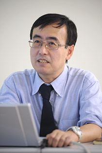
With the widespread adoption of wireless technology in mobile phones and wireless LAN, GPS, Bluetooth, ZigBee Sensor Network, Wireless USB, etc., high speed and high frequency circuits are rapidly gaining importance. However, if various wireless techniques are packed into a single mobile device, not only does it occupy a large circuit area, but also increases power consumption. Can’t we make the chips smaller like the digital circuits so that we can reduce power consumption, increase efficiency and cut down costs? Prof. Ishihara Noboru of Tokyo Institute of Technology’s Integrated Research Institute Solution Research Green ICT (Project leader - Prof. Masu Kazuya) is conducting a research on whether or not the size of wireless circuits can be reduced like the digital circuits.
Prof. Ishihara Noboru
“I aspire to create a RF (High Frequency) circuit that can be used in all wireless devices with just a basic circuit.” Digital circuits are becoming smaller and smaller, but it is impossible to reduce the size of analog circuits due to their passive electrical components such as coils (inductors).
But Prof. Ishihara is not ready to accept this fact. If analog circuits can become smaller like digital circuits, they will be more cost effective, consume less electricity and more efficient. If power consumption is reduced, battery life will naturally increase. What more do we need??
Cost can be reduced drastically if a common RF chip can be used for all wireless devices. This can be achieved through mass production. The application will be different from the present RFID. All products will have an RF chip. Attaching the chips to clothes and books does not only help prevent theft but also enable tracking of stolen goods! Portable devices that can download contents wirelessly will become very popular. One can even watch news on their wrist watch! Doctors will be able to monitor the body temperature, blood pressure, heart rate, etc. of their patients at any point in time.
Prof. Ishihara does not limit himself to the research on circuits. He is developing an actual product and experimenting on it. Otherwise, this will amount to nothing but only an empty theory that is of no use to the industry. As part of the new applications, a series of experiment has been carried out on a small PH sensor, which requires the cooperation of the enterprises to use it, send the measured value wirelessly to a receiver and then process with a computer. Prof. Ishihara says, “We still have to use a battery. But we are trying to make it batteryless.” This is what we call “Energy Harvester technology”.
Analog front end specialist
Prof. Ishihara is an expert in wireless circuit and has conducted research on optical communication, satellite communication and analog front end circuits of mobile wireless devices at NTT Electrical Communications Laboratories.
The miniaturization of analog circuits, which was the topic of Prof. Ishihara’s work, was a difficult task to achieve. When the specifications of the wireless circuits, especially coils (inductors) are determined, their size cannot be reduced. Prof. Ishihara wondered whether or not it is possible to make a wireless circuit without using coils. He thought of making an analog circuit with CMOS, which is usually used in digital circuits. CMOS can be miniaturized from 180nm to 130nm, 90nm, 65nm, 45nm and the entire signal amplitude can be utilized. Full swing high voltage CMOS devices are usually preferred, since miniaturization reduces noise resistance with the reduction in power voltage.
In addition, analog circuits had to be built depending on the applications. In the case of high frequency circuits, coils or capacitors were used for resonance and there was a fixed narrow frequency band for transceiving. “If the frequency band is wider, transceiving can be accomplished with a single basic circuit for various applications,” thought Prof. Ishihara and worked towards a broadband amplifier.
For the broadband amplifier which uses CMOS inverter configuration as the basis, he used CMOS to configure the Cherry- Hooper circuit which was conventionally made using bipolar circuits. But this would only mean that there is no feedback from the resistance. So, he installed an active feedback circuit with the CMOS inverter configuration. When active feedback is applied, negative feedback changes to positive since the phase rotates due to the parasitic capacity of the transistor at high frequency. Usually, the frequency characteristic shows that the gain decreases in high frequency region. But in this case, the gain increases in the high frequency region since there is a positive feedback and hence the bandwidth can also be increased.
Moreover, the local oscillation circuits required for heterodyne receivers also use CMOS. However, coils or capacitors were conventionally used for the resonance circuits. As mentioned earlier, we did not want to use coils. So ring oscillators were used. However, their characteristics showed that there was high phase noise. As a result, crystal oscillator injection locking was used instead, which is often seen in digital circuits. The phase noise reduces by 20 - 30dB in the experiment.
The wireless circuit chip designed by Prof. Ishihara also consists of an LDO (low drop out) power circuit which converts the voltage from the battery. Since miniaturization of this power transistor is not necessary, comprehensive knowledge is required to use these concept, such as increasing the gate length to double that of the inverter CMOS.
The low noise amplifier of CMOS which was developed as a test piece produced unprecedented results. The 180nm CMOS has the following specifications - power voltage: 1.8V, band: 0 – 4.9 GHz, power consumption: 30.6mW, gain: 30.6dB, noise: 3.5 – 4.7 dB and circuit area: 0.0067mm². And with the 90nm chip, the power voltage was 1.0V, the band was wider with 0 – 6.8 GHz, the power consumption was reduced to 14.5mW, the gain was reduced to 18.0dB, the noise of 3.0 – 5.5 dB was almost the same and the circuit area was less than half at 0.0032 mm².
Designing silicon IC s
Prof. Ishihara’s group is also undertaking IC design with EDA tools since they propose to give experimental proof by attaching their high frequency wireless circuit to a silicon chip. Designing starts at 180nm and then reduced to 90nm, 65nm, 45nm and so on. The process of attaching it to the actual silicon is done by an external manufacturing specialist. Presently, TSMC Taiwan manufactures the 90nm chip. The latest 65nm RF circuits that are being produced by VDEC, e-Shuttle, etc. are expected to be ready by mid-November.
They are designed with EDA tools, but the important thing is ‘to give an experimental proof of the circuit technology by actually manufacturing the product’. The search for a foundry for the 45nm process is still in progress since the shuttle service is not available yet.
Prof. Ishihara thinks that an overall design which includes LSI, module level, chassis level, etc. is required to construct a platform to design the RF circuits. There are plans to collaborate with well-established companies to construct such platforms.
The fundamentals of optical fibre, copper wire and wireless are the same
According to Prof. Ishihara, the fundamentals of transceiver circuits of optical fibers, wireless circuits and copper wire circuits are the same. Hence, he similarly wishes to design communication circuits with wireless radio, optical fiber and Ethernet cable. If this becomes possible, then the basic circuit can be used in various forms with minimal alteration.
In the case of wireless, since digital information is placed on a narrow band as the band is narrow, it is best to broaden digital information through direct current. There is little difference between optical and radio when it comes to widening the band.
Widespread use of wireless devices
If the single chip wireless circuit introduced by Prof. Ishihara becomes a reality, mobile phones, smart phones and smart books can made with a single chip and it can also be used for wireless software and cognitive wireless in the future. This will not only widen the application of global mobile devices, but also makes it possible to use wireless circuits in MP-3 players and digital cameras. It has an extensive scope of application.
Wireless circuits can be used for water quality examination if attached to a PH sensor


RS e-newsletters gives u the latest scoop at your convenience.
